Next: TIP850-10 (ADC/DAC, 12 Bit, Up: Hardware Previous: TIP551-10 (DAC, 16 Bit, Contents Index
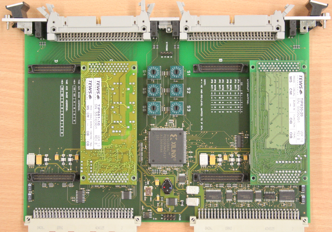
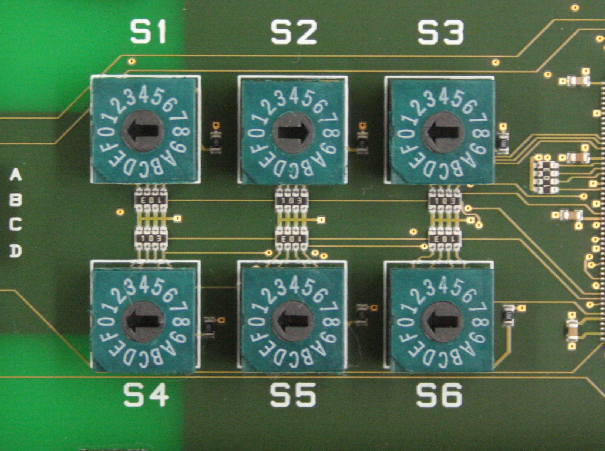
Carrier TVME200-10: S1 = 0, S2 = 8 (0x0800), S2 can be 0, 4, 8, C only, S4: A24/A32 memory enable and size, S4 = 0 - A24/A32 memory disabled, S4 = 1 - A24, 128 kB, 32 bK/IP, S4 = 2 - A24, 256 kB, 64 kB/IP, S5, S6: A24/A32 base address, def: 0xd00000 (A24), 0x00000000 (A32), S5: A[23:20], S6: A[19:16] for A24, S5: A[31:28], S6: A[27:24] for A32, memory must be boundary aligned with S4, power requirements: 300mA at 5V, 1 mA at +12V, 1mA at -12V (figures 65.1 and 65.2).
Carrier: VIPC616, A16D16 1k at 0x800 base (every piggy back uses 256B), base2 0x0. Jumpers: E3.7-E7.7 1111011 (from left to right, VME connectors point downwards), A24, E20.8-E21.8 11101111 (A23-A17, 0x10 00 00, parking position, avoids collisions with V260 I/Os), the other jumpers remain in the default position. VIPC616 power requirements: 0 mA at 12V, 0 mA at -12V, 610 mA at 5V.
The '1' of the ribbon cable is at the bottom of the TVME-200 connectors, at the left of the patch board connectors.
!
! '0x800' corresponds to position 'A'
!
 def adc1/module=tip830/dev=adc/base=0x800/chan=0
 def adc2/module=tip830/dev=adc/base=0x800/chan=1
 def adc3/module=tip830/dev=adc/base=0x800/chan=2
 def adc4/module=tip830/dev=adc/base=0x800/chan=3
 def adc5/module=tip830/dev=adc/base=0x800/chan=4
 def adc6/module=tip830/dev=adc/base=0x800/chan=5
 def adc7/module=tip830/dev=adc/base=0x800/chan=6
 def adc8/module=tip830/dev=adc/base=0x800/chan=7
Tango (/online_dir/online.xml):
<hw>
... other devices
<device>
 <name>exp_adc01</name>
 <type>adc</type>
 <module>tip830</module>
 <device>p09/adc/exp.01</device>
 <control>tango</control>
 <hostname>haso107tk:10000</hostname>
</device>
<device>
 <name>exp_adc02</name>
 <type>adc</type>
 <module>tip830</module>
 <device>p09/adc/exp.02</device>
 <control>tango</control>
 <hostname>haso107tk:10000</hostname>
</device>
<device>
 <name>exp_adc03</name>
 <type>adc</type>
 <module>tip830</module>
 <device>p09/adc/exp.03</device>
 <control>tango</control>
 <hostname>haso107tk:10000</hostname>
</device>
<device>
 <name>exp_adc04</name>
 <type>adc</type>
 <module>tip830</module>
 <device>p09/adc/exp.04</device>
 <control>tango</control>
 <hostname>haso107tk:10000</hostname>
</device>
<device>
 <name>exp_adc05</name>
 <type>adc</type>
 <module>tip830</module>
 <device>p09/adc/exp.05</device>
 <control>tango</control>
 <hostname>haso107tk:10000</hostname>
</device>
<device>
 <name>exp_adc06</name>
 <type>adc</type>
 <module>tip830</module>
 <device>p09/adc/exp.06</device>
 <control>tango</control>
 <hostname>haso107tk:10000</hostname>
</device>
<device>
 <name>exp_adc07</name>
 <type>adc</type>
 <module>tip830</module>
 <device>p09/adc/exp.07</device>
 <control>tango</control>
 <hostname>haso107tk:10000</hostname>
</device>
<device>
 <name>exp_adc08</name>
 <type>adc</type>
 <module>tip830</module>
 <device>p09/adc/exp.08</device>
 <control>tango</control>
 <hostname>haso107tk:10000</hostname>
</device>
</hw>
Figure 64.3 shows the combined resolution of the TIP551 (ADC) and TIP830-20 (ADC) as a function of voltage.